Overview
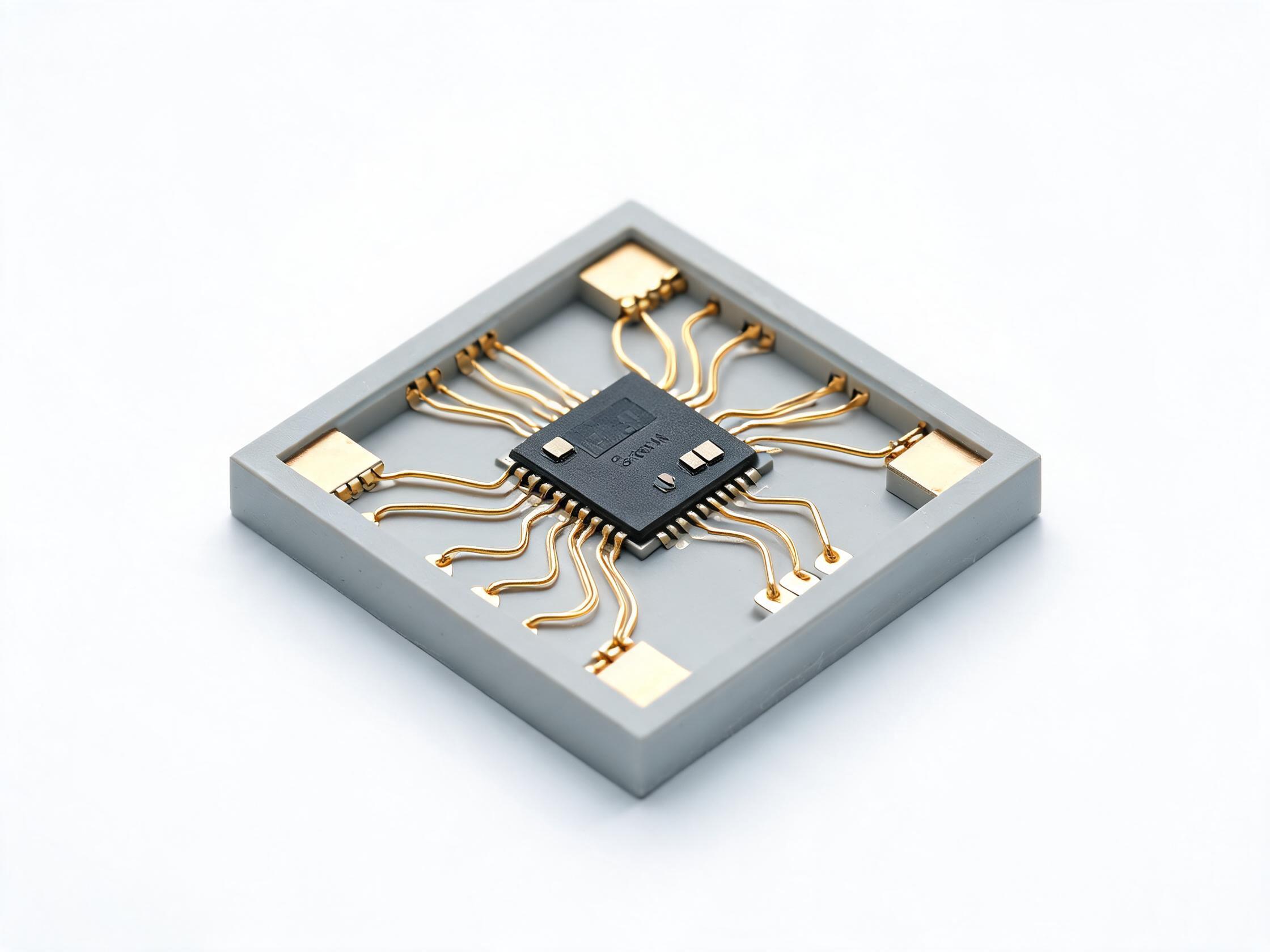
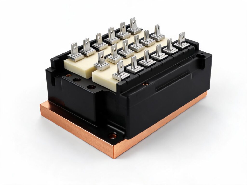
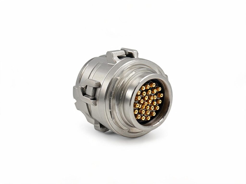
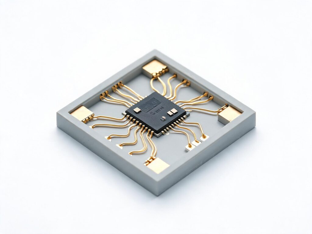
Gallium Arsenide (GaAs) and Gallium Nitride (GaN) RF semiconductor devices for high-frequency power amplification, radar, and communication systems. Our GaN devices offer superior power density, efficiency, and frequency performance compared to conventional technologies.
Key Features
- Wide bandgap GaN-on-SiC technology for high power density
- Excellent thermal conductivity for high-temperature operation
- High efficiency (up to 70% drain efficiency in Class AB)
- Broad frequency range from DC to millimeter wave
- Low parasitic capacitance and high breakdown voltage
- Available as bare die, packaged devices, and matched modules
Technical Specifications
| Parameter | Specification |
|---|---|
| Frequency Range | DC to 40 GHz (model-dependent) |
| Output Power | 0.5W to 100W (CW), up to 500W (pulsed) |
| Gain | 10 dB to 30 dB (linear) |
| Operating Voltage | 12V to 50V DC (drain bias) |
| Drain Efficiency | 40% to 70% (Class AB operation) |
| Package Type | Ceramic QFN, metal-ceramic flange, bare die |
| Thermal Resistance | 1.5°C/W to 5°C/W (junction-to-case) |
| Operating Temperature | -55°C to +150°C (Tj max) |
| Standards | MIL-PRF-38535, AEC-Q101 (automotive grade) |
Applications
- 4G/5G base station power amplifiers
- Radar systems (ground, air, naval)
- Satellite communication uplinks
- Electronic warfare (EW) systems
- ISM band heating and plasma applications
Contact us for detailed specifications and custom solutions.